The demand for general lighting market is growing day-by-day, which means that LED bulbs need to complement the lumen output of conventional halogen and incandescent bulbs.
The standard high-brightness (HB) LED merely converts about 45% of energy, while the rest 55% is given out as mere heat. Now, it is important to quickly remove heat from the LED in order to prevent overheating of the LEDs. This is known as thermal management that has been challenging the manufacturers of LEDs worldwide. On the brighter side, there exist a wide variety of ways that can solve this issue.
The effective solution to thermal management should start from LED packaging as it offers physical security to the LED die along with the technique to repair the LED onto the luminaire. However, at the same time, it also refers that LED die is then in a preserved enclosure, which mainly avertsheat loss by radiation and convection.
Owing to this fact, use of thermally conductive substrates has increased where they aid in reducing the thermal pathway between LEDs and heat sink. According to John Cafferkey, Marketing Manager, Cambridge Nanotherm, who has been quoted in a magazine, whilst it might be an easy alternative to employ something like a slab of copper for the work since copper is an extremely thermally conductive material, there is something more to it. The thermal substrate requires to be electrically insulating as it is also necessary to bear the copper tracks that carry electricity to the LED. In the absence of this dielectric, you might need to shorten the LED.
Hence, it is important for the LED industry to opt for that material which is thermally conductive but at the same time, as a dielectric as well.
Packaging alternatives
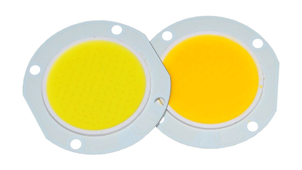
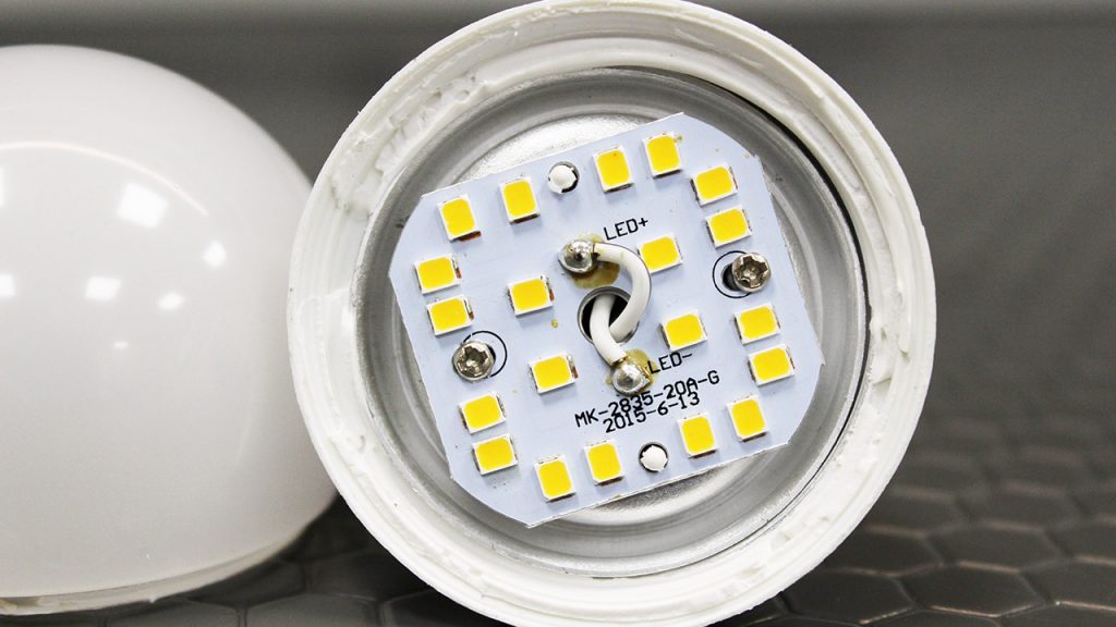
John Cafferkey says that there are two advancements to HB LED packaging. The LED manufacturers have the option to either package one big LED die or a collection die into a tool that can be accumulated with the help of surface-mount technology (SMT). On the other hand, they can package numerous die directly onto what is basically a printed-circuit board (PCB) – the chip-on-board (COB) advancement.
HB LEDs and advantages of ceramics
For directional HB LED packaging, both sides of the packaging substrate are required to be circuitized with copper tracks via the substrate offering link between the two sets of circuits. This requirement is significant since the packaging substrate will be mounted on top of a luminaire circuit responsible for providing power to the LED die.
To date, the only mass-market substance that was actually able to meet this need was electronics-grade ceramic. Ceramic is perfect since it is a natural dielectric and specific types of ceramic are adequately superior thermal conductors.
Nano Ceramic and its varied benefits
Nano ceramic materials have emerged as an effective option as they are known for bringing the best of ceramic and aluminum to the market. It is manufactured through a patented high-voltage electrochemical-oxidation (ECO) procedure. This coating measures only 10-30 μm, which is sufficient to act as a dielectric however its implication is that the combined thermal performance of the substance is extremely high at 152W/mK.
Also, nano ceramics overcome the two problems that prevent average MCPCBs from being used. Exclusively, it can be used to make isolated via holes in aluminum PCBs. Prior to going through the ECO method, the aluminum is drilled. Also, it includes the through-hole surfaces that are layered with a dielectric coating of nano ceramic. This helps to make a finished material with thermally competent, yet electrically isolating, through-holes that can be filled with copper to put up interconnects.
Briefly, it can be said that that thermal management of HB LEDs is not a simple task at all. Every design has to be examined and materials selected to complement the needs. The entire situation gets altered owing to nano ceramic that provides a material capable of establishing connection between 30W/mK and 170W/mK. Additionally, nano ceramics aid in overall cost reduction.
BizLED Magazine